- 您现在的位置:买卖IC网 > Sheet目录317 > C8051F380-TB (Silicon Laboratories Inc)DEV KIT FOR C8051F38X
�� �
�
�C8051F380/1/2/3/4/5/6/7/C�
�Master�
�Device�
�GPIO�
�MISO�
�MOSI�
�SCK�
�NSS�
�MISO�
�MOSI�
�SCK�
�NSS�
�MISO�
�MOSI�
�Slave�
�Device�
�Slave�
�Device�
�SCK�
�NSS�
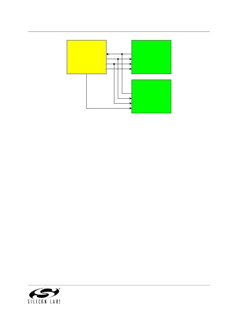
�Figure� 25.4.� 4-Wire� Single� Master� Mode� and� 4-Wire� Slave� Mode� Connection� Diagram�
�25.3.� SPI0� Slave� Mode� Operation�
�When� SPI0� is� enabled� and� not� configured� as� a� master,� it� will� operate� as� a� SPI� slave.� As� a� slave,� bytes� are�
�shifted� in� through� the� MOSI� pin� and� out� through� the� MISO� pin� by� a� master� device� controlling� the� SCK� sig-�
�nal.� A� bit� counter� in� the� SPI0� logic� counts� SCK� edges.� When� 8� bits� have� been� shifted� through� the� shift� reg-�
�ister,� the� SPIF� flag� is� set� to� logic� 1,� and� the� byte� is� copied� into� the� receive� buffer.� Data� is� read� from� the�
�receive� buffer� by� reading� SPI0DAT.� A� slave� device� cannot� initiate� transfers.� Data� to� be� transferred� to� the�
�master� device� is� pre-loaded� into� the� shift� register� by� writing� to� SPI0DAT.� Writes� to� SPI0DAT� are� double-�
�buffered,� and� are� placed� in� the� transmit� buffer� first.� If� the� shift� register� is� empty,� the� contents� of� the� transmit�
�buffer� will� immediately� be� transferred� into� the� shift� register.� When� the� shift� register� already� contains� data,�
�the� SPI� will� load� the� shift� register� with� the� transmit� buffer� ’s� contents� after� the� last� SCK� edge� of� the� next� (or�
�current)� SPI� transfer.�
�When� configured� as� a� slave,� SPI0� can� be� configured� for� 4-wire� or� 3-wire� operation.� The� default,� 4-wire�
�slave� mode,� is� active� when� NSSMD1� (SPI0CN.3)� =� 0� and� NSSMD0� (SPI0CN.2)� =� 1.� In� 4-wire� mode,� the�
�NSS� signal� is� routed� to� a� port� pin� and� configured� as� a� digital� input.� SPI0� is� enabled� when� NSS� is� logic� 0,�
�and� disabled� when� NSS� is� logic� 1.� The� bit� counter� is� reset� on� a� falling� edge� of� NSS.� Note� that� the� NSS� sig-�
�nal� must� be� driven� low� at� least� 2� system� clocks� before� the� first� active� edge� of� SCK� for� each� byte� transfer.�
�Figure� 25.4� shows� a� connection� diagram� between� two� slave� devices� in� 4-wire� slave� mode� and� a� master�
�device.�
�3-wire� slave� mode� is� active� when� NSSMD1� (SPI0CN.3)� =� 0� and� NSSMD0� (SPI0CN.2)� =� 0.� NSS� is� not�
�used� in� this� mode,� and� is� not� mapped� to� an� external� port� pin� through� the� crossbar.� Since� there� is� no� way� of�
�uniquely� addressing� the� device� in� 3-wire� slave� mode,� SPI0� must� be� the� only� slave� device� present� on� the�
�bus.� It� is� important� to� note� that� in� 3-wire� slave� mode� there� is� no� external� means� of� resetting� the� bit� counter�
�that� determines� when� a� full� byte� has� been� received.� The� bit� counter� can� only� be� reset� by� disabling� and� re-�
�enabling� SPI0� with� the� SPIEN� bit.� Figure� 25.3� shows� a� connection� diagram� between� a� slave� device� in� 3-�
�wire� slave� mode� and� a� master� device.�
�Rev.� 1.4�
�253�
�发布紧急采购,3分钟左右您将得到回复。
相关PDF资料
C8051F912DK
KIT DEV FOR C8051F91X/C8051F90X
C8051F930-TB
BOARD TARGET/PROTO W/C8051F930
C8051T610DB24
DAUGHTER BOARD T610 24QFN SOCKET
C8051T630DB20
BOARD SOCKET DAUGHTER 20-QFN
CAN-100
BOARD EVAL RS232 100QFP
CANADAPT28
KIT ADAPTER CANDEMOBOARD 28PLCC
CAT24AA01WI-GT3
IC EEPROM SERIAL 1KB I2C 8SOIC
CAT24AA02WI-G
IC EEPROM SERIAL 2KB I2C 8SOIC
相关代理商/技术参数
C8051F381
制造商:SILABS 制造商全称:SILABS 功能描述:USB DRIVER CUSTOMIZATION
C8051F381-GM
功能描述:8位微控制器 -MCU USB-64K-Flash
RoHS:否 制造商:Silicon Labs 核心:8051 处理器系列:C8051F39x 数据总线宽度:8 bit 最大时钟频率:50 MHz 程序存储器大小:16 KB 数据 RAM 大小:1 KB 片上 ADC:Yes 工作电源电压:1.8 V to 3.6 V 工作温度范围:- 40 C to + 105 C 封装 / 箱体:QFN-20 安装风格:SMD/SMT
C8051F381-GMR
功能描述:8位微控制器 -MCU USB-Flash-64k-ADC RoHS:否 制造商:Silicon Labs 核心:8051 处理器系列:C8051F39x 数据总线宽度:8 bit 最大时钟频率:50 MHz 程序存储器大小:16 KB 数据 RAM 大小:1 KB 片上 ADC:Yes 工作电源电压:1.8 V to 3.6 V 工作温度范围:- 40 C to + 105 C 封装 / 箱体:QFN-20 安装风格:SMD/SMT
C8051F381-GQ
功能描述:8位微控制器 -MCU USB-64K-Flash
RoHS:否 制造商:Silicon Labs 核心:8051 处理器系列:C8051F39x 数据总线宽度:8 bit 最大时钟频率:50 MHz 程序存储器大小:16 KB 数据 RAM 大小:1 KB 片上 ADC:Yes 工作电源电压:1.8 V to 3.6 V 工作温度范围:- 40 C to + 105 C 封装 / 箱体:QFN-20 安装风格:SMD/SMT
C8051F381-GQR
功能描述:8位微控制器 -MCU USB-Flash-64k-ADC RoHS:否 制造商:Silicon Labs 核心:8051 处理器系列:C8051F39x 数据总线宽度:8 bit 最大时钟频率:50 MHz 程序存储器大小:16 KB 数据 RAM 大小:1 KB 片上 ADC:Yes 工作电源电压:1.8 V to 3.6 V 工作温度范围:- 40 C to + 105 C 封装 / 箱体:QFN-20 安装风格:SMD/SMT
C8051F382
制造商:SILABS 制造商全称:SILABS 功能描述:USB DRIVER CUSTOMIZATION
C8051F382-GQ
功能描述:8位微控制器 -MCU USB-Flash-32k-ADC
RoHS:否 制造商:Silicon Labs 核心:8051 处理器系列:C8051F39x 数据总线宽度:8 bit 最大时钟频率:50 MHz 程序存储器大小:16 KB 数据 RAM 大小:1 KB 片上 ADC:Yes 工作电源电压:1.8 V to 3.6 V 工作温度范围:- 40 C to + 105 C 封装 / 箱体:QFN-20 安装风格:SMD/SMT
C8051F382-GQR
功能描述:8位微控制器 -MCU USB-Flash-32k-ADC RoHS:否 制造商:Silicon Labs 核心:8051 处理器系列:C8051F39x 数据总线宽度:8 bit 最大时钟频率:50 MHz 程序存储器大小:16 KB 数据 RAM 大小:1 KB 片上 ADC:Yes 工作电源电压:1.8 V to 3.6 V 工作温度范围:- 40 C to + 105 C 封装 / 箱体:QFN-20 安装风格:SMD/SMT